Introduction
PCB design software, or Printed Circuit Board design tools, are specialized programs that enable engineers and designers to create, simulate, and optimize electronic circuits on boards. These tools handle everything from schematic capture—drawing the electrical connections—to layout routing, where components are placed and traces are drawn, often including simulation for testing virtual prototypes and generating manufacturing files like Gerber outputs. Modern PCB software integrates 3D visualization, design rule checks (DRC), and collaboration features to ensure boards are functional, manufacturable, and compliant with standards.
Its importance cannot be overstated in the electronics industry, where miniaturization, high-speed signals, and reliability are key. By catching errors early through simulation and analysis, these tools reduce costly revisions, speed up time-to-market, and support innovation in devices like smartphones and EVs. With the rise of IoT, 5G, and AI hardware, PCB software helps manage complex multi-layer boards while optimizing for power efficiency and thermal management.
Key real-world use cases include consumer electronics for designing compact gadgets, automotive for robust ECUs in vehicles, aerospace for high-reliability avionics, medical devices for precise implants and monitors, and telecommunications for high-frequency RF boards. For example, a startup might use PCB software to prototype a wearable sensor, while a large firm simulates signal integrity in data center hardware to prevent failures.
When choosing PCB design software, users should evaluate based on criteria like schematic and layout capabilities, support for multi-layer and high-speed designs, integration with component libraries and MCAD tools, simulation features for signal integrity or thermal analysis, ease of generating manufacturing outputs, collaboration options for teams, and overall cost including licensing and training. Scalability for project complexity, cross-platform compatibility, and regular updates for new standards like IPC-2581 are also crucial.
Best for: Electronics engineers, hardware designers, and PCB layout specialists benefit most, along with hobbyists, educators, startups, SMBs, and enterprises in industries such as consumer electronics, automotive, aerospace, medical, and telecom. Solo makers appreciate free tools for quick prototypes, while large teams value enterprise features for collaboration and compliance.
Not ideal for: Pure software developers or non-electronics focused users might find basic diagramming tools like Visio sufficient. For highly specialized RF or analog simulations without PCB needs, standalone CAE software could be better, as full PCB suites might be overly complex and resource-heavy for simple sketches or non-manufacturing tasks.
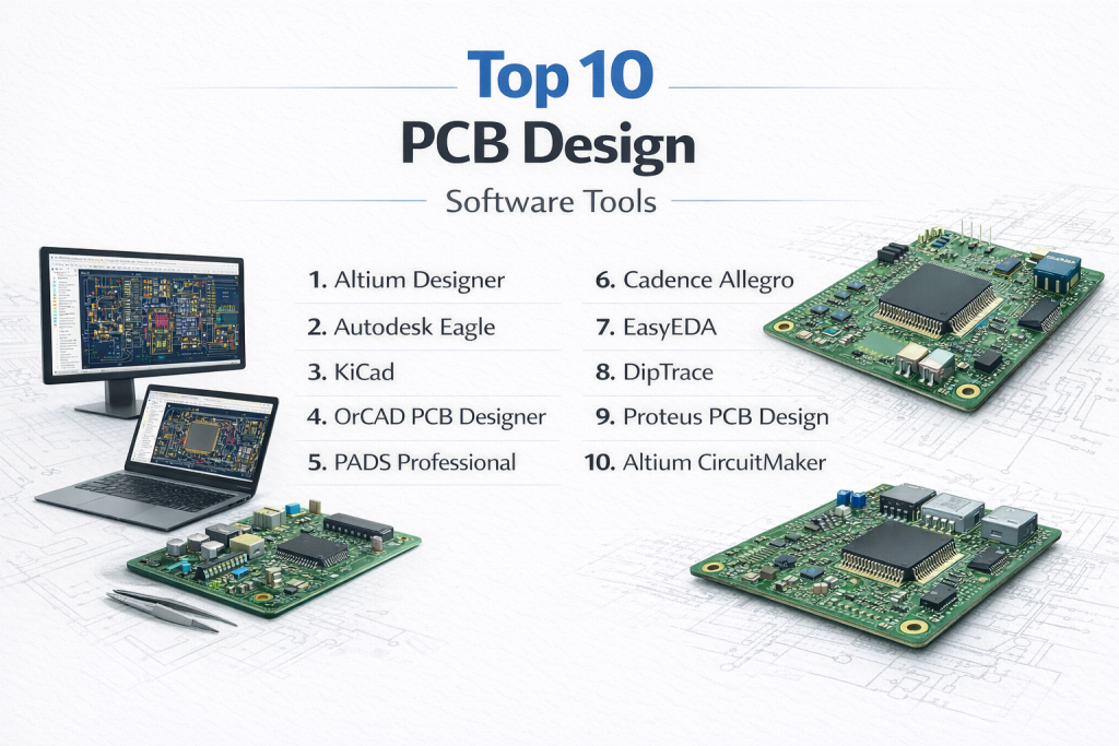
Top 10 PCB Design Software Tools
1 — Altium Designer
Altium Designer is a high-end, unified platform for professional PCB design, combining schematic capture, layout, simulation, and manufacturing preparation, designed for engineers handling complex, high-performance boards in enterprises.
Key features:
- Advanced interactive routing with push-and-shove for high-density boards.
- Integrated signal integrity, power analysis, and SPICE simulation.
- Extensive component libraries with supply chain integration.
- 3D visualization and MCAD co-design support.
- Real-time design rule checks and DFM validation.
- Automation for manufacturing outputs like Gerber and ODB++.
- Cloud collaboration via Altium 365 for team workflows.
Pros:
- Streamlines end-to-end design, reducing errors and iterations based on user feedback.
- Handles intricate multi-layer designs efficiently, ideal for aerospace and automotive pros.
- Strong ecosystem for scalability, praised by experts for reliability in production.
Cons:
- Steep learning curve for newcomers, requiring significant training time.
- High system resource demands, which can slow performance on average hardware.
- Expensive licensing, not budget-friendly for small teams or hobbyists.
Security & compliance: Role-based access control, data encryption, enterprise authentication; compliant with GDPR and ISO standards for regulated industries.
Support & community: Comprehensive documentation with tutorials and webinars; dedicated enterprise support with SLAs; large global user forums and training resources.
2 — Autodesk Eagle
Autodesk Eagle is a user-friendly PCB design tool integrated with Fusion 360, suited for makers, startups, and SMBs focusing on accessible schematic and layout workflows with mechanical integration.
Key features:
- Schematic editor with real-time synchronization to PCB layout.
- Autorouter and manual routing tools for efficient trace placement.
- Extensive community-driven component libraries.
- 3D modeling and cross-platform support (Windows, macOS, Linux).
- Design rule checking with customizable constraints.
- Integration with Autodesk Fusion for electro-mechanical design.
- Script automation via ULPs for custom workflows.
Pros:
- Intuitive interface lowers the barrier for beginners while scaling for pros.
- Cloud-based features enable seamless collaboration, valued by remote teams.
- Cost-effective for startups, with strong integration reducing workflow silos.
Cons:
- Limited advanced simulation compared to enterprise tools.
- Performance issues with very large or complex boards.
- Subscription model may add up over time for long-term use.
Security & compliance: Cloud access controls, data encryption in transit; GDPR-aligned; varies for enterprise deployments.
Support & community: Robust documentation and tutorials; active maker forums; commercial support through Autodesk.
3 — KiCad
KiCad is an open-source, free PCB design suite offering professional-grade tools for schematic capture and layout, ideal for hobbyists, educators, and budget-conscious professionals.
Key features:
- Full schematic capture with hierarchical sheets.
- Push-and-shove routing for multi-layer boards.
- 3D viewer for PCB inspection and export.
- Integrated SPICE simulator for circuit analysis.
- Unlimited layers and board size without restrictions.
- Cross-platform compatibility and open library system.
- Design rule checks and Gerber file generation.
Pros:
- Completely free with no feature limits, enabling broad access.
- Community-driven updates keep it evolving, as noted in expert reviews.
- Reliable for educational and small-scale production use.
Cons:
- Less polished UI than commercial alternatives, potentially frustrating users.
- Manual library management can be time-consuming.
- Lacks built-in advanced high-speed design tools.
Security & compliance: N/A (primarily local desktop tool); varies with self-hosted setups.
Support & community: Extensive forums, tutorials, and wikis; highly active global community; no formal enterprise support.
4 — OrCAD PCB Designer
OrCAD is a professional PCB tool from Cadence, focused on constraint-driven design for high-reliability applications, designed for mid-to-large teams in regulated sectors.
Key features:
- Advanced schematic capture with multi-page support.
- Constraint manager for high-speed and RF designs.
- Signal integrity analysis and simulation.
- Integrated component and library management.
- DFM and DRC for manufacturing readiness.
- Seamless upgrade path to Allegro for complex projects.
- Millions of CAD symbols and 3D models available.
Pros:
- Robust for critical systems, ensuring compliance and reliability.
- Intuitive for beginners yet scalable, per user consensus.
- Strong integration with enterprise workflows.
Cons:
- Outdated interface in some aspects, feeling less modern.
- Higher costs limit accessibility for small users.
- Steeper curve for advanced features.
Security & compliance: Enterprise security controls; compliant with GDPR, ISO; suitable for regulated environments like medical.
Support & community: Professional documentation; Cadence support with SLAs; dedicated user groups.
5 — PADS Professional
PADS Professional, part of Siemens, is a scalable PCB design solution emphasizing advanced layout and analysis, tailored for engineering teams in mid-to-large organizations.
Key features:
- High-speed routing with visual tracking.
- Integrated signal and power integrity simulations via HyperLynx.
- Thermal analysis and design constraints.
- Flexible licensing for standard to professional versions.
- Comprehensive documentation and schematic tools.
- Manufacturing outputs and supply chain insights.
- Multi-user collaboration capabilities.
Pros:
- Balances cost and features for growing teams.
- Reliable for high-density designs, as highlighted in industry reports.
- Excellent customer support from Siemens.
Cons:
- Complex setup for beginners.
- Outdated GUI in places.
- Not as affordable for solo users.
Security & compliance: Role-based access, data encryption; SOC 2, GDPR compliant.
Support & community: Outstanding documentation; enterprise support; professional networks.
6 — Cadence Allegro
Cadence Allegro is a high-end suite for complex, high-density PCB designs, suited for large enterprises dealing with HDI and RF applications.
Key features:
- Advanced constraint management for high-speed signals.
- AI-based auto-placement and routing.
- Signal, power, and thermal integrity analysis.
- DFM/DFT validation tools.
- Scalable for team environments.
- Pre/post-layout simulations.
- Flexible workspace customization.
Pros:
- Handles intricate designs with precision, reducing failures.
- Efficient error correction and analysis, per expert views.
- Ideal for telecom and aerospace reliability.
Cons:
- Overwhelming for small projects or beginners.
- High licensing costs.
- Limited backward compatibility.
Security & compliance: SSO, encryption, audit logs; ISO, GDPR compliant.
Support & community: Detailed guides; Cadence enterprise support; industry forums.
7 — EasyEDA
EasyEDA is a cloud-based tool for quick PCB prototyping, perfect for hobbyists, startups, and small teams needing browser-accessible design and manufacturing integration.
Key features:
- Online schematic and layout editor.
- Integrated component sourcing from LCSC.
- Direct fabrication links to JLCPCB.
- Versioning and collaboration in the cloud.
- DRC and Gerber export.
- Free tier with paid upgrades.
- Cross-device accessibility.
Pros:
- No installation needed, enabling rapid starts.
- Seamless design-to-manufacture flow, saving time.
- Affordable for entry-level users.
Cons:
- Relies on internet, limiting offline work.
- Fewer advanced features for complex boards.
- Performance varies with connection.
Security & compliance: Cloud encryption, access controls; GDPR varies by plan.
Support & community: Forums and tutorials; basic support.
8 — DipTrace
DipTrace offers intuitive PCB design with professional tools, aimed at SMBs and independent engineers balancing ease and capability for multi-layer boards.
Key features:
- Hierarchical schematics and autorouting.
- 3D visualization and STEP export.
- Real-time DRC and component editor.
- Import/export for various formats.
- Multi-sheet design support.
- Affordable tiered pricing.
- Clean interface for faster workflows.
Pros:
- Easy to learn, boosting productivity for mid-level users.
- Good value with polished features.
- Responsive support appreciated by users.
Cons:
- Limited for ultra-high-speed designs.
- Smaller community than open-source peers.
- Not as widely adopted in large industries.
Security & compliance: N/A (desktop-focused).
Support & community: Good docs; customer support; moderate forums.
9 — Proteus PCB Design
Proteus combines PCB layout with advanced simulation, ideal for embedded systems designers needing real-time testing of microcontroller circuits.
Key features:
- Integrated schematic and MCU simulation.
- Manual and auto-routing with length matching.
- Extensive component models for analog/digital.
- 3D visualization and export.
- Differential pair routing.
- Fast simulation engine.
- Large library for embedded projects.
Pros:
- Reduces physical prototyping costs through simulation.
- User-friendly for education and pros.
- Strong for firmware-integrated designs.
Cons:
- Less advanced layout for non-embedded use.
- Commercial licensing required.
- Limited collaboration.
Security & compliance: N/A.
Support & community: Documentation; academic/professional base; commercial help.
10 — Altium CircuitMaker
Altium CircuitMaker is a free, community-driven tool based on Altium’s engine, for makers and open-source projects emphasizing collaboration and professional routing.
Key features:
- Schematic and PCB layout with advanced routing.
- Community libraries and project sharing.
- Cloud storage and collaboration.
- Up to 16 layers support.
- 3D visualization.
- Gerber and ODB++ outputs.
- Fusion 360 integration.
Pros:
- Professional features at no cost for public projects.
- Encourages community innovation.
- Intuitive for electrical circuits.
Cons:
- Requires public sharing for full use.
- No offline saving without internet.
- Instability in complex simulations.
Security & compliance: Secure cloud storage; public constraints.
Support & community: Active forums; growing user base.
Comparison Table
| Tool Name | Best For | Platform(s) Supported | Standout Feature | Rating |
|---|---|---|---|---|
| Altium Designer | Enterprise complex designs | Windows | Unified schematic-to-manufacture | N/A |
| Autodesk Eagle | Startups and makers | Windows, macOS, Linux | Real-time sync with Fusion 360 | N/A |
| KiCad | Budget-conscious pros | Windows, macOS, Linux | Open-source unlimited layers | N/A |
| OrCAD PCB Designer | Regulated high-reliability | Windows | Constraint-driven simulation | N/A |
| PADS Professional | Mid-to-large teams | Windows | Signal integrity with HyperLynx | N/A |
| Cadence Allegro | High-density HDI boards | Windows, Linux | AI auto-placement and analysis | N/A |
| EasyEDA | Rapid online prototyping | Web-based | Integrated sourcing and fabrication | N/A |
| DipTrace | SMB intuitive designs | Windows, macOS | Hierarchical schematics with 3D | N/A |
| Proteus PCB Design | Embedded MCU simulation | Windows | Real-time firmware testing | N/A |
| Altium CircuitMaker | Open-source collaboration | Windows, Cloud | Community-driven libraries | N/A |
Evaluation & Scoring of PCB Design Software
To score these tools, we used industry consensus from user reviews and expert analyses, rating each category on a 1-10 scale. Overall scores are weighted averages.
| Tool Name | Core Features (25%) | Ease of Use (15%) | Integrations & Ecosystem (15%) | Security & Compliance (10%) | Performance & Reliability (10%) | Support & Community (10%) | Price / Value (15%) | Overall Score |
|---|---|---|---|---|---|---|---|---|
| Altium Designer | 9 | 7 | 9 | 8 | 9 | 9 | 7 | 8.3 |
| Autodesk Eagle | 8 | 9 | 8 | 7 | 8 | 8 | 8 | 8.1 |
| KiCad | 8 | 8 | 7 | 5 | 8 | 9 | 10 | 8.0 |
| OrCAD PCB Designer | 9 | 7 | 8 | 9 | 9 | 8 | 6 | 8.0 |
| PADS Professional | 8 | 7 | 8 | 8 | 9 | 8 | 7 | 7.9 |
| Cadence Allegro | 9 | 6 | 8 | 9 | 9 | 7 | 5 | 7.7 |
| EasyEDA | 7 | 9 | 7 | 7 | 7 | 7 | 9 | 7.7 |
| DipTrace | 7 | 9 | 6 | 5 | 8 | 7 | 8 | 7.4 |
| Proteus PCB Design | 8 | 8 | 7 | 5 | 8 | 7 | 7 | 7.4 |
| Altium CircuitMaker | 7 | 8 | 7 | 6 | 7 | 8 | 10 | 7.6 |
Which PCB Design Software Tool Is Right for You?
Picking the right PCB design software starts with your setup and goals. For solo users or hobbyists, free options like KiCad or Altium CircuitMaker provide robust tools without costs, allowing experimentation on personal projects like Arduino boards. These are great for learning and small prototypes where simplicity trumps enterprise features.
SMBs and mid-market companies often need a mix of affordability and scalability—tools like Autodesk Eagle or DipTrace fit here, offering intuitive interfaces for teams of 5-50, with collaboration to handle growing product lines like IoT devices. They support multi-user edits without overwhelming complexity.
Enterprises with large teams should go for premium suites like Altium Designer, Cadence Allegro, or PADS Professional, which excel in handling massive, high-stakes designs with simulations for compliance in sectors like automotive. These include HPC support and integrations for PLM systems.
If budget is tight, prioritize value-driven free or low-cost tools like EasyEDA or DesignSpark PCB, which deliver core functions for rapid prototyping without subscriptions. For premium investments, OrCAD or Proteus justify costs with advanced analysis, saving on revisions in the long run.
Weigh feature depth against ease: Beginners favor EasyEDA’s browser access over Allegro’s power. For integration, choose Eagle for MCAD or Altium for supply chains; scalability matters for expanding from single boards to fleets. If security is paramount—like in medical or defense—opt for compliant tools with SSO and encryption, such as OrCAD or PADS, to protect IP and meet GDPR/ISO.
Frequently Asked Questions (FAQs)
What is PCB design software? It’s specialized software for creating electronic circuit boards, including schematic drawing, component placement, routing traces, and preparing files for manufacturing.
Why use PCB design software over manual methods? It automates error checking, simulations, and optimizations, reducing costs and time while ensuring reliability in complex designs.
How much does PCB design software cost? Ranges from free (KiCad, EasyEDA) to subscriptions ($500+/year for Eagle) or perpetual licenses ($5,000+ for Altium), depending on features.
Is PCB software secure for sensitive designs? Many offer encryption and access controls; enterprise tools like OrCAD comply with GDPR and ISO, but check for your needs.
Can PCB tools scale for large projects? Yes, enterprise options like Allegro handle multi-layer HDI boards; start small and upgrade as complexity grows.
What are common implementation hurdles? Learning curves and hardware requirements; begin with tutorials and trial versions to ease onboarding.
Are there free alternatives to paid tools? KiCad and CircuitMaker provide professional features without costs, ideal for non-commercial use.
What mistakes do new users make? Ignoring DRC early or poor library management; always validate rules and organize components from the start.
Best practices for PCB design? Use hierarchical schematics, simulate before layout, collaborate via version control, and focus on DFM for smooth manufacturing.
How does simulation fit in? It tests circuits virtually for issues like signal integrity, preventing real-world failures and iterations.
Conclusion
This deep dive into the top 10 PCB design software showcases a vibrant market, from free open-source gems like KiCad to powerhouse enterprise solutions like Altium Designer and Cadence Allegro. Key takeaways include the push toward integrated simulation, cloud collaboration, and AI-assisted routing, helping designers tackle denser, faster boards in evolving industries.
What truly matters in choosing is matching the tool to your workflow—consider complexity, team size, budget, and compliance needs above all. There’s no single “best” winner; success depends on your specific projects, whether prototyping a gadget or engineering avionics. Test options through free trials, weigh long-term value, and select one that empowers efficient, innovative designs.